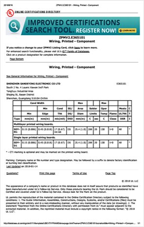
Blind-buried Vias PCB
6L Blind-buried Vias PCB
Blind Vias start on an outer layer but terminate on an inner layer. Buried Vias exist only between inner layers and do not begin or terminate on an outer layer.
Blind and buried vias are particularly advantageous in HDI PCBs because they optimize the density of the boards without increasing board size or the number of board layers you require.
Send Inquiry >