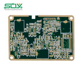
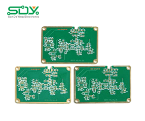
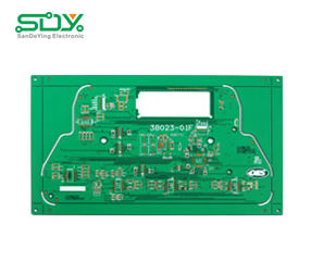
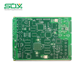
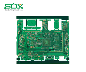
Blind-buried Vias PCB
Blind Vias start on an outer layer but terminate on an inner layer. Buried Vias exist only between inner layers and do not begin or terminate on an outer layer.
Blind and buried vias help to save PCB real estate by allowing features and lines to be designed above or below them without making a connection. Many of today’s fine pitch BGA and flip-chip component footprints do not allow for running traces between the BGA pads. Blind and buried vias will only connect layers requiring connections in that area.
- Total 1 Pages 7 Records

