• 2L LCB Module PCB

Bonding PCB

2L LCB Module PCB

Wire bonding is the method of making interconnections (ATJ) between an integrated circuit (IC) or other semiconductor device and its packaging during semiconductor device fabrication. Although less common, wire bonding can be used to connect an IC to other electronics or to connect from one printed circuit board (PCB) to another.

Wire bonding is generally considered the most cost-effective and flexible interconnect technology and is used to assemble the vast majority of semiconductor packages. If properly designed, wire bonding can be used at frequencies above 100 GHz.

Send Inquiry >
Basic Information
Layer 2L
Base Material FR4
Board thickness 1.6mm
Copper weight 1Oz
Surface finish Immersion Gold
Application LCD Module Products
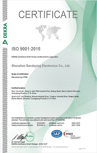
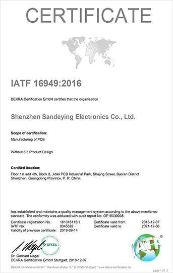
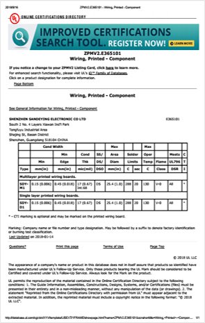
Certificate UL, ISO9001, TS16949, RoHS
Additional Information
Brand SDY
Origin Shenzhen, China
Packing Inner Bubble Pack + Standard Carton
Payment Terms T/T
Transportation Ocean, Land, Air
- -
- -

Application

There are multiple challenges when it comes to wire bond manufacturing and reliability. These challenges tend of be a function of several parameters such as the material systems, bonding parameters, and use environment. Different wire bond-bond pad metal systems such as Aluminum-Aluminum (Al-Al), Gold-Aluminum (Au-Al), and Copper-Aluminum (Cu-Al) require different manufacturing parameters and behave differently under the same use environments.

Bonding PCB board normally used for a various products but not limited to: consumer electronics, telecommunication, planar transformers, aerospace, military and so on.

PCB capability and services


  • 1

    Single-sided, double side & multi-layer PCB. FPC. Flex Rigid PCB with competitive price, good quality and excellent service

  • 2

    CEM-1, FR-4, FR-4 High TG, Aluminum base material, Polyimide, Rogers, Taconic etc

  • 3

    HAL, HASL, Immersion Gold, Immersion Silver, Plating Gold, Plating Nickel, Plating Silver, Gold Finger, OSP surface treatment

  • 4

    Quantities range from sample to mass order100% E-Test

Our Advantages

  • Certification

    ISO 9001 and UL certificate

  • Technology

    Comprehensive technical support from design to manufacture

  • Innovation

    High technology supported by continuous investment

  • Profession

    More than 10 years experiences in the production of PCB

  • Team

    Professional oversea sales team with over 5years working experiences

  • Service

    Excellent after-sell service

  • What We Need ?

    Gerber files / PCB files

    Pcb sepecification: base material; board thickness; copper thickness; color of solder mask and silkscreen; surface finished

    Quantity and Time requirement

  • Freight and Payment

    By DHL, UPS, FedEx, TNT using clients account.

    We suggest you using our DHL, UPS, FedEx, TNT forwarder.

    By EMS (Usually for Russia Clients), price is high.

    By sea for mass quantity according to customer's requirement.

    By customer's Forwarder.

    By Paypal, T/T, West Union, etc.

  • PCB Production Time

    1-2Layers : sample: 2-3 days / mass production: 7-8 days

    Multi-layer : sample: 5-6 days / mass production: 8-10 days

    Special board : 2 weeks / mass production: 2 weeks

  • ISO certificate

  • ISO certificate

  • ISO certificate

Inquiry Now!
Inquiry Now!

© 2019 Shenzhen SanDeYing Electronic Co., Ltd | All Right Reserved | Design by Gemelsoft.