• 4-Layer Gold Finger PCB

Gold Finger PCB

4-Layer Gold Finger PCB

Gold Finger PCB refers to those PCBs with finger-like pads applying plated gold surface finish, and they are usually used as edge-connectors.

Electroless gold gives excellent solderability, but the chemical deposition process means that it is too soft and too thin to withstand repeated abrasion. Electroplated gold is thicker and harder making it ideal for edge-connector contacts for PCBs which will be repeatedly plugged in and removed.

Gold Finger PCBs normally have to bevel the edge connectors to ensure easy insertion. Bevelling can be specified in the order details if there are any special instructions.

Send Inquiry >
Basic Information
Layer 4L
Base Material FR4
Board thickness 1.6mm
Copper weight 1Oz
Surface finish Lead free HASL + Gold Finger
Application Medical Equipment
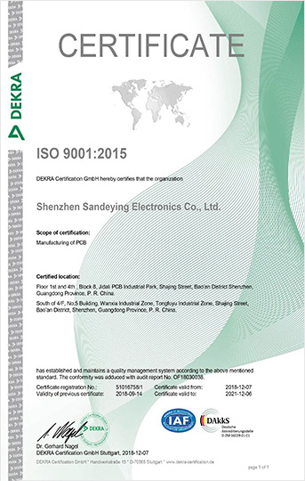
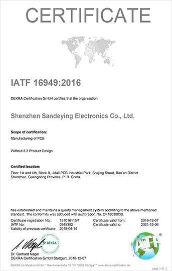
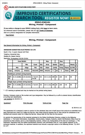
Certificate UL, ISO9001, TS16949, RoHS
Additional Information
Brand SDY
Origin Shenzhen, China
Packing Inner Bubble Pack + Standard Carton
Payment Terms T/T
Transportation Ocean, Land, Air
- -
- -

Application

The application of gold fingers to an edge connector provides an ideal surface finish for high-wear applications, such as an insertion connector. This is partly due to the fact that hardened gold provides a very planar surface that is resistant to wear from repeated insertions. For the manufacture of printed circuit boards, a bright hard gold with a mixture of nickel and/or cobalt is often used for card edge connector fingers plated over a nickel underlayment.

PCB capability and services


  • 1

    Single-sided, double side & multi-layer PCB. FPC. Flex Rigid PCB with competitive price, good quality and excellent service

  • 2

    CEM-1, FR-4, FR-4 High TG, Aluminum base material, Polyimide, Rogers, Taconic etc

  • 3

    HAL, HASL, Immersion Gold, Immersion Silver, Plating Gold, Plating Nickel, Plating Silver, Gold Finger, OSP surface treatment

  • 4

    Quantities range from sample to mass order100% E-Test

Our Advantages

  • Certification

    ISO 9001 and UL certificate

  • Technology

    Comprehensive technical support from design to manufacture

  • Innovation

    High technology supported by continuous investment

  • Profession

    More than 10 years experiences in the production of PCB

  • Team

    Professional oversea sales team with over 5years working experiences

  • Service

    Excellent after-sell service

  • What We Need ?

    Gerber files / PCB files

    Pcb sepecification: base material; board thickness; copper thickness; color of solder mask and silkscreen; surface finished

    Quantity and Time requirement

  • Freight and Payment

    By DHL, UPS, FedEx, TNT using clients account.

    We suggest you using our DHL, UPS, FedEx, TNT forwarder.

    By EMS (Usually for Russia Clients), price is high.

    By sea for mass quantity according to customer's requirement.

    By customer's Forwarder.

    By Paypal, T/T, West Union, etc.

  • PCB Production Time

    1-2Layers : sample: 2-3 days / mass production: 7-8 days

    Multi-layer : sample: 5-6 days / mass production: 8-10 days

    Special board : 2 weeks / mass production: 2 weeks

  • ISO certificate

  • ISO certificate

  • ISO certificate

Inquiry Now!
Inquiry Now!

© 2019 Shenzhen SanDeYing Electronic Co., Ltd | All Right Reserved | Design by Gemelsoft.