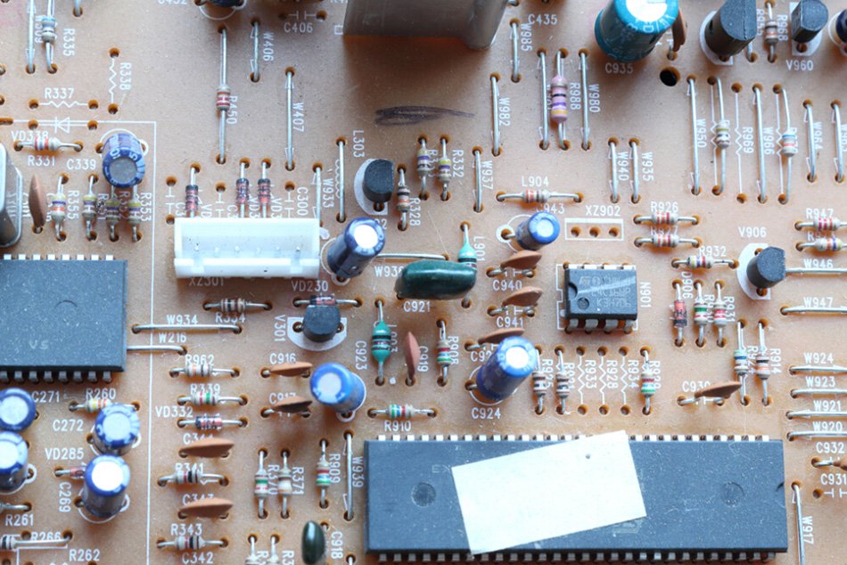
How to Design PCB Silkscreens to Ensure Usability
Silkscreen designs may range from very simple to quite complicated. It is just as common to not make sufficient use of this opportunity to provide identification and markings to aid your board’s assembly as it is to include too much information. However, following the simple guidelines below will help you make the best use of your silkscreen.

Design Guidelines for PCB Silkscreens
1. Determine which process your CM uses to create silkscreens
Most CMs will not utilize all three of the silkscreen processes; therefore, you should find out what method your CM implements. This will impact your design in terms of size, clearances, and location of silkscreen markings and other elements, such as component pads, traces, and vias.
2. Account for silkscreen items during PCB layout
For readability, markings such as polarity, pin one, and reference indicators need to be as close to the associated components as possible. These additional real estate requirements should be considered as you are creating your layout to ensure there is no overlap or covering of the indicators.
3. Choose fonts based on CM’s method
Some PCB design packages allow you to create virtually any font style for your silkscreen. However, the number of fonts that your CM can produce may be much more restricted. You should consult with your CM to ensure that you are incorporating fonts that can actually be generated on your board.
4. Do not overuse silkscreen markings
It can be tempting to include indicators for all components and include other informational imagery that may be helpful for assembly, testing, or repair of your board. However, with the ongoing evolution towards smaller and densely packed PCBs, this is probably not possible. Therefore, you should prioritize the markings that you include as follows:
- Regulatory requirements; such as lead-free labeling required by J-STD-609A Marking and Labeling of Components, PCBs and PCBAs to Identify Lead (Pb), Lead-Free (Pb-Free) and Other Attributes from IPC.
- Manufacturer identification; including markings such as board part number, serial number, labels, and the logo.
- Assembly aids; such as polarity and pin one indicators. Reference indicators should be used based on available space.
- Testing aids; such as test point indicators, mode and/or jumper indicators.
Following the guidelines above on how to design PCB silkscreens will help you make the best use of identification and labeling on your board.
